Chapter 2
Operational Amplifiers
Having just been introduced to several aspects of circuit simulation using Spice, we are now ready to re-enforce our understanding of linear circuits constructed with Operational Amplifiers. We shall begin our investigation by developing a simple voltage-controlled voltage-source (VCVS) representation of the op amp from which to study various types of op amp circuits. Progressively, we shall increase the complexity of the op amp model in order to capture more of the true-life behavior and the effect that this behavior has on closed-loop circuit operation. Several new Spice concepts will be discussed here; largely in order to describe the nonlinear circuit behavior of an op amp to Spice.
2.1 Modeling an Ideal Op Amp with Spice
An ideal op amp as shown in Fig. 2.1 may be modeled as a voltage-controlled voltage source with infinite voltage gain (i.e., A ® ¥). The input resistance is very high, infinite in fact, and the output resistance is considered to be zero since the output node is driven directly by a voltage source. Moreover, the voltage gain is assumed to be independent of frequency. At a first glance, a Spice model for the ideal op amp may seem to be trivial - a one-line VCVS Spice statement. Unfortunately, Spice has no concept of infinity, hence, the infinite voltage gain cannot be specified as a Spice value. Instead, we must compromise the accuracy of our ideal model by specifying a large, but finite, voltage gain value. Normally, a value of 106 V/V is sufficient without any significant deviation from the ideal. Under this gain condition, we shall consider the op amp as pseudo-ideal.
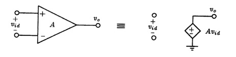
Fig. 2.1: Equivalent circuit of the ideal op amp (A ® ¥).
2.2 Analyzing the Behavior of Ideal Op Amp Circuits
We have now come to a point where we can use Spice to analyze the behavior of various types of op amp circuits, and thus develop a better understanding of these circuits.
2.2.1 Inverting Amplifier
Consider the inverting op amp circuit shown in Fig. 2.2 which consists of one ideal op amp and two resistors R1 and R2. We would like to determine the DC transfer function of this circuit when R1 and R2 assume values of 1 k ohm and 10 k ohm, respectively.
To perform this calculation using Spice we shall make use of the Transfer Function (.TF) command briefly discussed in the last chapter. The syntax of this command was not discussed there, rather we shall present it here and use it to analyze the op amp circuit shown in Fig. 2.2.
The transfer-function analysis command of Spice computes the DC small-signal gain from the input of a circuit driven by some signal source to some pre-specified network variable. In addition, this command will also calculate the input resistance of the circuit as seen by the input source, and the output resistance seen looking back into the circuit from the port formed by the output variable and ground. Alternatively, this command can be viewed as calculating the Thevenin or Norton equivalent circuit of the network from the point-of-view of the input and output ports.
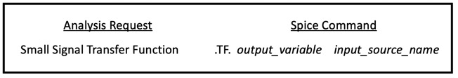
Table 2.1: Small-signal transfer function analysis request.
A general description of the syntax of the Transfer Function analysis command (.TF) is given in Table 2.1. The different fields of this command should be self-evident from the discussion above. The command line begins with the keyword .TF followed by the output variable, either a voltage at a node or a current through a voltage source, and the name of the input signal source for which the output will be referenced to. The results of the .TF command are directly sent to the Spice output file in much the same way as that performed previously by the .OP command. No .PRINT or .PLOT statement is required in the Spice input file in order to view the results of the .TF command.
|
Fig. 2.2 The inverting amplifier circuit.
|
Inverting Amplifier Configuration ** Circuit Description ** * signal source Vi 3 0 DC 1v * inverting amplifier circuit description R1 3 2 1k R2 2 1 10k Eopamp 1 0 0 2 1e6 ** Analysis Requests ** .TF V(1) Vi ** Output Requests ** * none required .end
Fig. 2.3: Spice input deck for calculating the small-signal characteristics of the circuit shown in Fig. 2.2.
|

Returning to the circuit shown in Fig. 2.2, one can create the Spice input file shown in Fig. 2.3. Here the op amp is modeled as a VCVS with a voltage gain of 106 V/V. A one-volt DC signal is applied to the input of the circuit and a .TF analysis request was included to compute the DC small-signal voltage gain.
The results of the Transfer Function calculations, as produced by Spice, are listed below together with the small signal bias solution:
|
**** SMALL SIGNAL BIAS SOLUTION TEMPERATURE = 27.000 DEG C
NODE VOLTAGE NODE VOLTAGE NODE VOLTAGE NODE VOLTAGE
( 1) -9.9999 ( 2) 10.00E-06 ( 3) 1.0000
**** SMALL-SIGNAL CHARACTERISTICS
V(1)/Vi = -1.000E+01 INPUT RESISTANCE AT Vi = 1.000E+03
OUTPUT RESISTANCE AT V(1) = 0.000E+00
|
Clearly, the voltage gain from the DC input source to the op amp output of -10 as calculated by Spice agrees with the expected voltage gain determined by the ratio - R2 / R1. In addition, the input and output resistances are listed. Combining this information with that of the gain calculation allows us to represent the op amp circuit of Fig. 2.2 with the equivalent circuit model shown in Fig. 2.4.
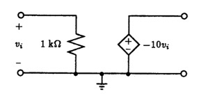
Fig. 2.4: Equivalent circuit model of the inverting amplifier configuration of Fig. 2.2 as calculated by Spice.
Evident in the ``SMALL SIGNAL BIAS SOLUTION'' is that the negative terminal of the op amp (node 2) is not exactly at ground potential. This error is caused by the finite DC gain used to model the terminal behavior of the ideal op amp and would be expected to decrease with increasing the op amp DC gain. In most practical cases, an error of this magnitude is considered insignificant and need not be a cause for alarm.
|
Fig. 2.5: The Miller Integrator.
|
The Miller Integrator ** Circuit Description ** * signal source Vi 3 0 PWL (0 0V 1ms 0V 1.001ms 1V 10ms 1V) * components of the Miller integrator R1 2 3 1k C2 2 1 10uF Eopamp 1 0 0 2 1e6 ** Analysis Requests ** .TRAN 100us 5ms 0ms 100us ** Output Requests ** .PRINT TRAN V(3) V(1) .probe .end
Fig. 2.6: Spice input deck for computing the step response of the circuit shown in Fig. 2.5.
|

The Miller Integrator
Our next example illustrates another important application of the inverting op amp configuration. Consider replacing R2 in the inverting amplifier circuit shown in Fig. 2.2 with a capacitor C2. The resulting configuration is known as the inverting or Miller integrator circuit and is shown in Fig. 2.5. Here we wish to determine the transient response of a Miller integrator with R1=1 k-ohm and C2=10 uF subject to a 1-volt step-input. On completion of this, we would also like to determine its AC frequency response.
The Spice input file used to calculate the transient response of the Miller Integrator is given in Fig. 2.6. At this point of the text most statements contained in this file should be self-explanatory; however, we need to clarify the description provided for realizing the step input. An ideal step function does not exist in Spice, so we need to approximate the step with a series of piece-wise linear segments. The pulse is held low at 0 V for 1 ms and then made to rise to 1 V with a rise-time of 1 us, and then held at 1 V for 9 ms. If the rise time of this pulse was made equal to zero then we would have realized a step function exactly; unfortunately, Spice will not accept a waveform having a rise-time of zero. Alternatively, we could decrease the rise time of the step input and more closely approximate the step function; however, this only increases the time to complete a simulation. For this particular example, a rise-time of 1 us was found to be sufficient.
The results of the transient simulation are shown in Fig. 2.7. The top curve represents the input step signal and the bottom curve represents the output of the integrator. Clearly, the output is the time-integral of the input, i.e., the integral of a step function is a ramp function. The rate at which the ramp output decreases is -400 mV/4 ms or -100 V/s. The magnitude of this rate can easily be shown to be equal to VI/C2R1 where VI is the magnitude of the input step. It should then be obvious why this circuit is called an integrator.
The AC frequency response of this circuit can be easily computed using Spice by simply changing the input source in the Spice input file of Fig. 2.6 from a time varying PWL voltage source to an AC voltage source with the following syntax:
Vi 3 0 AC 1V.
In addition, we must replace the .TRAN statement by an .AC statement specifying the range of frequencies that we are interested in. For this particular case, we are interested in a fairly broad frequency range of 1 Hz to 1 kHz, thus we decided to use a log sweep of the input frequency using the following .AC analysis statement:
.AC DEC 5 1Hz 1kHz.
The AC frequency response of the Miller integrator as calculated by Spice is displayed in Fig. 2.8. The magnitude of the output node voltage (V(1)) is large at low frequencies and rolls-off at a rate of -20 dB for each decade increase in frequency. Using the Probe post-processor available with PSpice, we found that the frequency at which the magnitude of the output voltage crosses the 0-dB level is 15.9 Hz. This corresponds exactly with the result of substituting the circuit parameters into the expression 1/ (2p R1C2).
|
Fig. 2.7: Step response of the Miller integrator circuit shown in Fig. 2.5 when R1 = 1 k ohm and C2 = 10 uF.
|
Fig. 2.8: Frequency response of the Miller integrator circuit shown in Fig. 2.5 when R1 = 1 k ohm and C2 = 10 uF.
|


A Damped Miller Integrator
The DC instability of a Miller integrator is a result of the very high (ideally infinite) DC gain that the Miller integrator has. The DC gain can be made finite by connecting a feedback resistor across integrating capacitor C2. Unfortunately, however, this makes the integrator nonideal, known as a damped integrator. To obtain near ideal response over a large frequency range the feedback resistor should be as large as possible.
In the following we shall investigate the behavior of a damped integrator for two different-sized feedback resistors. Specifically, we shall compare the step response of a damped integrator with feedback resistors of 1 M-ohm and 100 k-ohm to that of an ideal integrator. The Spice input file for each case is quite similar to that seen in Fig. 2.6 for the Miller integrator except for the following changes. The amplitude of the input step is reduced to 1 mV from the original 1-V level. This is to keep the output signal level within practical limits (i.e., between typical power supply levels). The element statement for this step input signal would then appear as follows:
Vi 3 0 PWL ( 0 0V 1ms 0V 1.001ms 1mV 2s 1mV ).
Secondly, the element statement for the feedback resistor is added to the Spice deck. For the case of 1 M-ohm feedback resistor, we would add the following statement:
R2 1 2 1Meg
and in the case of the 100 k-ohm feedback resistor we would add:
R2 1 2 100k.
A separate Spice deck is created for each case and concatenated together into one file. This will enable us to graphically compare the final results on a single graph using the Probe post-processing facility available in PSpice.
As the final change, the transient analysis command statement is changed to read as follows:
.TRAN 100ms 2s 0s 100ms.
To make direct comparisons with the ideal-integrator step-response, we shall also add the Spice deck for the Miller integrator shown in Fig. 2.6 (with the appropriate changes made) to the file containing the two Spice decks of damped integrators. For reference, we list the complete file containing the three Spice decks in Fig. 2.9. Notice that no space separates the end of one Spice deck, denoted by .end, and the start of the next one. If this is not adhered to, then the file will probably be rejected by Spice[1].
Spice version 2G6 and later have a built-in command called .ALTER that allows the user to specify changes to the circuit without having to re-type the entire file as we do here. Unfortunately, the student version of PSpice does not have this command or one that accomplishes the same thing, so we have opted to re-create a new Spice deck for each circuit change and concatenate them together into one file for processing. In this way, we can view the results together using Probe.
Submitting this input file to Spice for processing, results in the three step responses shown in Fig. 2.10; one result is for the ideal integrator and the other two are for the different damped integrators. Up to about 0.1 s, all three step responses are almost identical. After this, the integrator that is damped with 100 kW begins to deviate from the other two. Moreover, as the time progresses, the curve corresponding to this one begins to settle towards -100 mV. In the case of the 1 MW damped integrator, similar behavior is also observed but with a different time scale. The step response of this integrator begins to significantly deviate from the ideal after about 1 s. Although not shown, if we were to have the transient response calculation of Spice run longer, we would see the step response of this integrator settle to a -1 V level.
In either of the two damped integrator cases, we see that the step response deviates significantly from the ideal situation in about one-tenth the time-constant formed by the integrating capacitor C2 and the damping resistor R2 (i.e., C2R2/10). We can therefore conclude that the output of a damped integrator behaves much like an ideal integrator for times less than one-tenth the time constant formed by the feedback capacitor and resistor.
It is also interesting to observe the magnitude response behavior of the two damped integrators as a function of frequency and compare it to that obtained for the Miller integrator. Consider adding the following AC source statement and analysis command to each Spice input deck described in Fig. 2.9:
|
Vi 3 0 AC 1V .AC DEC 5 1mHz 1kHz.
|
On completion of the AC analysis, we obtain the results shown in Fig. 2.11. In contrast to the results of the ideal integrator, the two damped integrators have a magnitude response that consists of two parts: A low frequency component that is essentially independent of frequency and a second component that rolls off linearly with frequency at a rate of -20 dB/dec. The frequency point that divides the two regions is approximately the reciprocal of the time-constant formed by the feedback resistor and capacitor (i.e., 1/(2pC2R2)).
For frequencies about ten-times larger than the corresponding break or 3 dB frequency of the damped integrator, both the ideal and the damped integrator have essentially identical frequency response behavior. Thus, for input signal frequencies larger than 10 times the 3-dB frequency of the damped integrator, the response of the damped integrator closely approximates that of the ideal Miller integrator.
|
Fig. 2.5: The Miller Integrator. (duplicate)
|
The Miller integrator
** Circuit Description ** * signal sources Vi 3 0 PWL (0 0V 1ms 0V 1.001ms 1mV 2s 1mV) * components of the Miller integrator R1 2 3 1k C2 2 1 10uF Eopamp 1 0 0 2 1e6 ** Analysis Requests ** .TRAN 100ms 2s 0ms 100ms ** Output Requests .PLOT TRAN V(1) .probe .end The Damped Miller integrator (R=1M)
** Circuit Description ** * signal sources Vi 3 0 PWL (0 0V 1ms 0V 1.001ms 1mV 2s 1mV) * components of the Miller integrator R1 2 3 1k R2 1 2 1Meg C2 2 1 10uF Eopamp 1 0 0 2 1e6 ** Analysis Requests ** .TRAN 100ms 2s 0ms 100ms ** Output Requests .PLOT TRAN V(1) .probe .end The Damped Miller integrator (R=100k)
** Circuit Description ** * signal sources Vi 3 0 PWL (0 0V 1ms 0V 1.001ms 1mV 2s 1mV) * components of the Miller integrator R1 2 3 1k R2 1 2 100k C2 2 1 10uF Eopamp 1 0 0 2 1e6 ** Analysis Requests ** .TRAN 100ms 2s 0ms 100ms ** Output Requests .PLOT TRAN V(1) .probe .end
Fig. 2.9: The complete Spice deck for computing the step response of the two damped integrator circuits and one ideal integrator circuit. It consists of three separate Spice decks concatenated into one file.
|
|
Fig. 2.10: Comparing the 1 mV step response of two differently damped integrator circuits with that of an ideal Miller integrator circuit.
|
Fig. 2.11: Comparing the magnitude response behavior of two damped integrator circuits with that of an ideal Miller integrator. |


The Unity-Gain Buffer
This next example will repeat the same DC transfer function analysis performed above for the inverting amplifier on a unity-gain buffer. Although, the circuit itself will not prove very challenging for Spice, it will be used to highlight an apparent problem with Spice and the technique used to alleviate it.
Consider the unity-gain buffer shown in Fig. 2.12. The output of the op amp is feed directly back to its negative terminal and the input signal generator vi is connected to the positive terminal. The Spice input file for this circuit is listed in Fig. 2.13 and, on submission to Spice, the following results are found in the output file (excluding the input circuit description):
ERROR: Less than 2 connections at node 2
ERROR: Less than 2 connections at node 1
Obviously, something went wrong. Spice is complaining about having less than 2 connections at nodes 1 and 2. This is a topological restriction imposed by Spice in order to guarantee that the solution calculated is a unique one. Prior to the start of any simulation, Spice performs a topological check during the equation formulation phase to ensure that this restriction is not violated. If it is, then Spice reports in the output file the nodes that violate this condition.
On counting the number of connections made at nodes 1 and 2, there appears to be exactly two connections. So why then does Spice complain? The answer lies in the fact that Spice does not consider the input port of a voltage-controlled dependent source as an element. To eliminate this problem and have Spice get on with the circuit simulation, one must ``fool'' Spice into thinking that it has at least 2 connections at nodes 1 and 2. A very elegant solution is to connect zero-valued current sources between node 1 and ground, and node 2 and ground. In this way each current source acts as an open circuit and has no effect on the operation of the circuit. Alternatively, one could connect high-valued resistors between each node in question and ground. If the resistors added are large enough relative to other resistors in the circuit, then their presence will be insignificant.
|
Fig. 2.12: The unity-gain buffer.
|
Unity-Gain Buffer ** Circuit Description ** * signal source Vi 2 0 DC 1V * op-amp in unity-gain configuration Eopamp 1 0 2 1 1e6 ** Analysis Requests ** .TF V(1) Vi ** Output Requests ** * none required .end
Fig. 2.13: Spice input deck for calculating the DC small-signal gain of the circuit shown in Fig. 2.12. Spice rejects this file because of the lack of two connections at nodes 1 and 2.
Unity-Gain Buffer ** Circuit Description ** * signal source Vi 2 0 DC 1V * op-amp in unity-gain configuration Eopamp 1 0 2 1 1e6 Iopen1 1 0 0A ; redundant current-sources to eliminate Iopen2 2 0 0A ; less-than-two connection at nodes 1 and 2 ** Analysis Requests ** .TF V(1) Vi ** Output Requests ** * none required .end
Fig. 2.14: Revised Spice input deck for the unity-gain buffer shown in Fig. 2.12. Also included is two zero-valued current sources to rid the circuit of its less than 2 connections problem at nodes 1 and 2.
|

For the above example we added two zero-valued current sources. One between node 1 and ground, and the other between node 2 and ground. The revised Spice input file including these zero-valued current sources is listed in Fig. 2.14 and the small-signal characteristics, as calculated by Spice, are shown below:
|
**** SMALL SIGNAL BIAS SOLUTION TEMPERATURE = 27.000 DEG C
NODE VOLTAGE NODE VOLTAGE NODE VOLTAGE NODE VOLTAGE
( 1) 1.0000 ( 2) 1.0000
**** SMALL-SIGNAL CHARACTERISTICS
V(1)/Vi = 1.000E+00
INPUT RESISTANCE AT Vi = 1.000E+12
OUTPUT RESISTANCE AT V(1) = 0.000E+00
|
Notice that the input resistance of the unity-gain buffer is not infinite as it should be, but rather 1012 ohm. This is an artifact of the algorithm used by Spice to calculate the DC bias solution of a network. For all practical purposes, in a circuit such as the one shown in Fig. 2.12, one can consider a resistance value of 1012 ohm as being equivalent to a value of infinity.
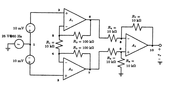
Fig. 2.15: A two-stage three op amp instrumentation amplifier.
Instrumentation Amplifier
Our next example is a two-stage instrumentation amplifier shown in Fig. 2.15 consisting of three op amps. Such an amplifier is usually employed as the front-end of an instrument that measures a differential signal between the amplifier input terminals (20 mV in Fig. 2.15). We would like to investigate the effect of a 60 Hz common-mode signal on such a measurement, as shown in Fig. 2.15. This example involves more op amps than previous examples; however, it does not pose any special difficulty for Spice. Any difficulty will usually be experienced by the user in the amount of effort that's required to type the correct circuit description into a computer file. In general, as more information has to be typed there exists a greater chance of entering erroneous data.
To simplify matters, and reduce the chances of error, a provision has been made in Spice for defining subcircuits. A subcircuit is considered separate and isolated from the main circuitry except that it is connected to the main circuit through specific nodes. Such a subcircuit can, of course, be used repeatedly in the same main circuit. This concept is analogous to the subroutine concept found in most computer programming languages such as FORTRAN. Experience has shown that Spice input files are easier to read, and simpler to debug, when a large circuit is described using subcircuits. In addition, once a subcircuit is created for a specific building block, it can be re-used by other circuits constructed from the same building blocks. Thus, subcircuits provide a convenient way of creating a library of basic building blocks for future use.
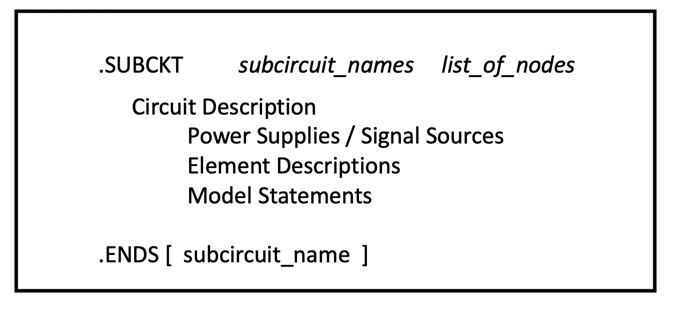
Fig. 2.16: Subcircuit format and syntax.
The format and syntax of a subcircuit definition is displayed in Fig. 2.16. It begins by a .SUBCKT statement followed by a unique name and a list of the internal nodes of the subcircuit that will be allowed to connect to the main circuit. Subsequent statements are used to describe the subcircuit to Spice in exactly the same way as that performed for the main circuit. The nodes of the subcircuit are local to the subcircuit and can have the same numbers as those used in the main circuit or any other subcircuit. One exception is the ground node (node 0) which is common to all circuits. Similarly, the names of the elements making up the subcircuit are also local to the subcircuit and can be the same as those used for other elements in the main circuit. To conclude the definition of the subcircuit, the final statement must be an .ENDS statement. Notice that this includes an ``S'' appended on its end to distinguish it from an end to the Spice input file. The name of the subcircuit may also be included on the same .ENDS statement to clearly mark the end of the subcircuit.
Once a subcircuit has been defined it can be incorporated into the main circuit in much the same way as a circuit element is described to Spice. The beginning of the statement is a unique alphanumeric name prefixed with the letter ``X'' followed by a list of the nodes of the subcircuit that connect it to the main circuit. The final field must then specify the name of the subcircuit that is being referenced. Obviously, there must be a one-to-one correspondence between the list of nodes given on this statement and the ones listed on the .SUBCKT statement. For quick reference, the syntax of this statement is displayed in Fig. 2.17.
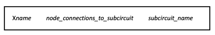
Fig. 2.17: Accessing a subcircuit by the main circuit.
Now returning to the instrumentation amplifier displayed in Fig. 2.15 we see that it consists of three identical op amps A1, A2 and A3. These can be conveniently described to Spice using the subcircuit facility. Consider the op amp equivalent circuit displayed in Fig. 2.1 and the following corresponding subcircuit description:
|
.subckt ideal_opamp 1 2 3 * connections: | | | * output | | * +ve input | * -ve input Eopamp 1 0 2 3 1e6 Iopen1 2 0 0A ; redundant connection made at +ve input terminal Iopen2 3 0 0A ; redundant connection made at -ve input terminal .ends ideal_opamp
|
One element statement is used to specify the VCVS and the other two are used to make redundant circuit connections at the floating nodes of the VCVS. Notice also that we added a set of comment statements clarifying the list of nodes that interface the subcircuit and the main circuit. One should always include such a description in every subcircuit for easy reference.
Each op amp of the instrumentation amplifier can now be described to Spice using the following subcircuit calls:
|
Xop_A1 6 2 5 ideal_opamp Xop_A2 7 3 4 ideal_opamp Xop_A3 10 9 8 ideal_opamp
|
The complete Spice input file including the op amp subcircuit for the instrumentation amplifier is on display in Fig. 2.18. In order to determine whether the 60 Hz common-mode signal is affecting the DC measurement being performed by the instrumentation amplifier, a transient analysis is to be performed by Spice.
On completion of Spice, we observe (Fig. 2.19) that the voltage waveform appearing at the output of the instrumentation amplifier (node 10) is a constant DC signal of 420 mV, even though the voltage appearing at the inputs of the instrumentation amplifier (nodes 2 and 3) are time-varying voltage waveforms riding on the very small DC signal of 10 mV. Comparing the DC level found at the output with that predicted by the equation derived by Sedra and Smith 3rd Edition in Example 2.5 of Section 2.6 for the instrumentation amplifier and repeated here below with the constraint R2=R3, R4=R5 and R6=R7:
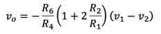
one finds that we are in perfect agreement when the appropriate component values are substituted. There is no evidence of the 60 Hz common-mode signal at the output. This highlights an important feature of the instrumentation amplifier; its ability to reject common-mode signals while amplifying much smaller difference signals.
|
Fig. 2.15: A two-stage three op amp instrumentation amplifier. (duplicate)
|
Instrumentation Amplifier
* op-amp subcircuit .subckt ideal_opamp 1 2 3 * connections: | | | * output | | * +ve input | * -ve input Eopamp 1 0 2 3 1e6 Iopen1 2 0 0A ; redundant connection made at +ve input terminal Iopen2 3 0 0A ; redundant connection made at -ve input terminal .ends ideal_opamp
** Main Circuit ** * signal sources Vcm 1 0 SIN (0 25V 60Hz) Vdc1 1 2 DC 10mV Vdc2 3 1 DC 10mV * instrumentation amplifier Xop_A1 6 2 5 ideal_opamp Xop_A2 7 3 4 ideal_opamp Xop_A3 10 9 8 ideal_opamp R1 5 4 10k R2 5 6 100k R3 4 7 100k R4 6 8 10k R5 7 9 10k R6 9 0 10k R7 8 10 10k ** Analysis Requests ** .TRAN 0.1ms 66.68ms 0 0.1ms ** Output Requests ** .PRINT TRAN V(2) V(3) V(10) .probe .end
Fig. 2.18: Spice input deck for calculating the transient response of the instrumentation amplifier shown in Fig. 2.15.
|

In the above simulation we assumed that the appropriate pairs of resistors (R4, R5, R6 and R7) were perfectly matched. In practise, this is rarely the case and, as a result, the lack of matching will affect the common-mode rejection capability of the instrumentation amplifier. To illustrate this, consider altering one of the resistors of the difference amplifier, say R5, by 1% of its nominal value. In other words, we shall repeat the above simulation with R5 having a value of 10.1 k-ohm. On doing so, one finds at the output of the instrumentation amplifier a 250-mV peak-to-peak 60 Hz frequency component riding on a DC level of 420 mV. The actual simulation result for the output waveform is displayed in Fig. 2.20. Clearly, the common-mode signal is now present at the output. This illustrates the importance of having closely matched resistors in the difference amplifier portion of the instrumentation amplifier.
|
Fig. 2.19: Input and output signals of the instrumentation amplifier. Notice that no AC signal is appearing at the output (V(10)) even though it is present at the two input nodes (V(2) and V(3)).
|
Fig. 2.20: The output voltage signal of the instrumentation amplifier when there is a 1% mismatch between R5 and R6 in the difference amplifier of Fig. 2.15.
|


2.3 Nonideal Op Amp Performance
In previous sections we performed several Spice simulations assuming that the op amps used had a very large open loop gain and that the gain was independent of frequency. In the remainder of this chapter we shall incorporate more of the nonidealities of practical monolithic op amps into our simulations; thus, obtaining results that are more realistic of closed-loop op amp behavior. Rather than simulate detailed op amp circuitry at the transistor level, which, of course, is a very feasible approach provided one has the knowledge of the internal circuit (Chapter 10), in this section we shall develop an equivalent circuit representation for the op amp that relies only on the information found on the manufacturer's data sheet.
Op amp nonidealities can be incorporated into the op amp circuit model in various ways. One method involves constructing a circuit whose terminal behavior provides a close resemblance to actual op amp terminal behavior. Obviously, one tries to find a simple circuit that captures the op amp nonideal behavior. Alternatively, with newer versions of Spice, specifically PSpice, terminal behavior can be specified using a mathematical expression in either functional or piecewise-linear form. This new approach to circuit modeling has come to be known as analog behavior modeling and forms a very elegant and powerful means of specifying nonlinear circuit behavior. We shall utilize this approach below to investigate the effect of large-signal properties of an op amp on the closed-loop response of op amp circuits. For the small-signal performance we shall use a lumped circuit model (an equivalent circuit) to represent the frequency response of the op amp.
2.3.1 Small-Signal Frequency Response of Op Amp Circuits
The differential small-signal open-loop gain of an internally compensated op amp can be mathematically described as
(2.1)
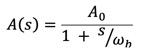
where A0 denotes the DC gain and wb is the 3-dB break frequency. Typically, A0 is very large, on the order of 106 V/V for modern bipolar op amps such as the 741 op amp and wb typically ranges between 1 and 100 rad/sec. The single-capacitor circuit shown in Fig. 2.21 has infinite input resistance and zero output resistance, much like the ideal op amp, and it can be shown that it has the following single-pole transfer function:
(2.2)
Clearly, if we let GmR1 = A0 and R1C1 = 1/wb, then the circuit shown in Fig. 2.21 can be used to model the small-signal frequency response of the op amp in Spice. As an example, consider typical frequency response parameters for the 741 op amp: it has a DC gain of 2.52 x 10⁵ V/V and a 3 dB frequency of 4 Hz. Using the above equations, we can write two equations in terms of three unknowns. Thus, we have at our disposal a single degree of freedom which we can exercise to obtain the other two circuit parameters. That is, if we let C=30 pF then we can solve for Gm= 0.190 mA/V and R1= 1.323 x 10⁹ W.
It is imperative that one check that the op amp model behaves as expected otherwise false conclusions would later be drawn. We shall perform this check in conjunction with our next example where we investigate the effects that the limited op amp gain and bandwidth have on the closed-loop gain of an inverting amplifier.
|
Fig. 2.21: A one-pole circuit representation of the small-signal open-loop frequency response of an internally compensated op amp.
Fig. 2.2 The inverting amplifier circuit. (duplicate)
|
Inverting Amplifier With Gain -1
* op-amp subcircuit .subckt small_signal_opamp 1 2 3 * connections: | | | * output | | * +ve input | * -ve input Ginput 0 4 2 3 0.19m Iopen1 2 0 0A ; redundant connection made at +ve input terminal Iopen2 3 0 0A ; redundant connection made at -ve input terminal R1 4 0 1.323G C1 4 0 30p Eoutput 1 0 4 0 1 .ends small_signal_opamp
** Main Circuit ** * signal source Vi 3 0 AC 1V 0Degrees Xopamp 1 0 2 small_signal_opamp R1 3 2 1k R2 2 1 1k ** Analysis Requests ** .AC DEC 5 0.1Hz 100MegHz ** Output Requests ** .PRINT AC V(3) V(1) .probe .end
Fig. 2.22: The Spice input deck for investigating the small-signal frequency response behavior of the inverting amplifier shown in Fig. 2.2 having a gain of -1. Other Spice decks can be appended to the end of this one to enable one to compare results with Probe.
|

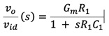
Consider calculating the frequency response of the inverting amplifier shown in Fig. 2.2 for nominal gains of -1, -10, -100 and -1000 using the one-pole op amp model calculated above. Furthermore, we will want to contrast the frequency response obtained in these four closed-loop cases with the open-loop response of the op amp using Probe. This is easily done by simply concatenating the Spice input decks into one file and submitting this larger file to Spice as if it were a single job. The results of all the analyses would then be found in one Spice output file or, for our purposes here, be accessible by Probe to graphically display and compare. Rather than list the entire contents of this input file because of its excessive length, we list only the Spice description for the inverting amplifier having a gain of -1 and the subcircuit used to represent the op amp, in Fig. 2.22. The Spice description for the other amplifiers would be identical to this one, except that R2 would change to reflect the gain required in each case. Also included in this concatenated file is a Spice description for computing the open-loop frequency response of the op amp (i.e., from the circuit of Fig. 2.2 with R1 shorted and R2 removed).
The frequency response behavior of the inverting amplifier under different gain settings is displayed in Fig. 2.23 together with the op amp open loop frequency response. One sees clearly the effect of increasing amplifier gain on its bandwidth. Moreover, the gain and bandwidth are seen not to exceed those values of the open-loop frequency response.
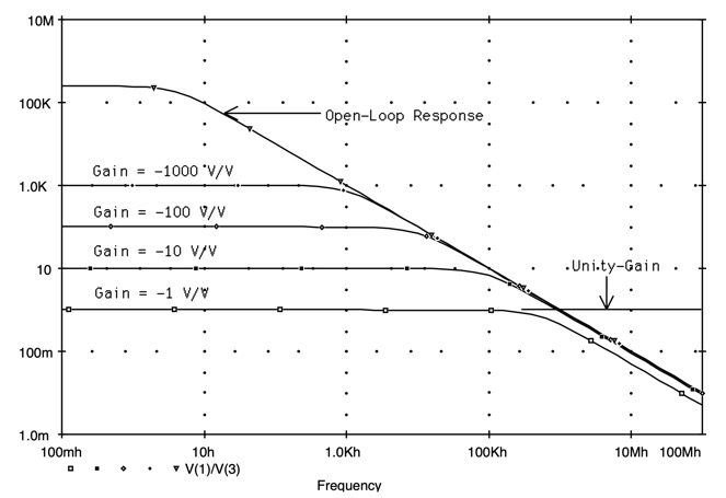
Fig. 2.23: Frequency response of an inverting amplifier having nominal closed-loop gains of -1, -10, -100 and -1000. Also shown is the open-loop frequency response of the op amp used in the inverting amplifier (A0=2.52 x 10⁵ V/V and fb=4 Hz).
2.3.2 Modeling the Large-Signal Behavior of Op Amps[2]
The above subcircuit model for the op amp is limited to circuit situations where the output voltage of the op amp is small. In this section we shall elaborate on the op amp subcircuit so that it can be used to model op amp behavior when subjected to both small and large input signals. To accomplish this, consider that the internal structure of an actual op amp consists of three parts as shown in Fig. 2.24 in contrast to the single stage model put forth above in the last subsection. The front-end stage consists of a differential-input transconductance amplifier, followed by a high gain voltage amplifier with gain -m, together with a feedback compensation capacitor C, and the final stage is simply an output unity-gain buffer providing a low output resistance. By modeling the terminal behavior of each stage of the op amp, accommodating both linear and nonlinear behavior, realistic op amp characteristics can be captured by Spice without simulating detailed internal circuitry.
To describe the behavior of these three stages to Spice, we make use of the equivalent circuit shown in Fig. 2.25. Here the gain of each dependent sources is expressed as an unspecified function of the controlling signal. The gains of these stages are written this way in order to convey to the reader that both the linear and nonlinear behavior of each of the internal stages is to be captured by these dependent sources. Spice has provisions for specifying nonlinear dependent sources; however, the functional description must be expressible in polynomial form. Unfortunately, this makes specifying arbitrary functions difficult. Instead, newer versions of Spice, specifically PSpice, allow users to specify the control function as a mathematical expression or in piecewise-linear form. We shall elaborate on this further below.
|
Fig. 2.24 Block diagram of the internal structure of an internally compensated op amp.
|
Fig. 2.25: Equivalent circuit representation of the internal behavior of an internally compensated op amp. In the small-signal region of the op amp i(vid)=Gmvid, v(vi2) = -v vi2, and v(vo2)=vo2.
|


Limited Current-Output of The Front-End Transconductance Stage
The first stage of an op amp is a circuit that converts a differential input voltage signal into a corresponding current. The operation of this stage is largely linear with transconductance Gm; however, the maximum output current that it can source or sink is limited to a value Imax. Conversely, the transconductance stage will behave linearly provided the input voltage levels are restricted to lie within the range -Imax/Gm to Imax/Gm. To help the reader visualize these transfer characteristics we display them in Fig. 2.26. Now to try and capture this behavior with a set of polynomials would be very difficult, if not, impossible. Instead, it can be very easily incorporated into the circuit representation using the analog behavior modeling capability of PSpice.
Fig. 2.26: Transfer characteristic of the input transconductance amplifier of an op amp.
The analog behavior model feature of PSpice is a set of extensions made to the VCVS and VCCS statements. These extensions allow the user to specify the controlled signal (voltage or current) in terms of the controlling variable (again, voltage or current) as either a mathematical expression or in piecewise-linear form. For example, the level of a VCCS with its output terminals connected between node 2 and ground can be made dependent on the square of the input voltage V(1) by simply using the following PSpice description,
Gsquare 2 0 VALUE = { V(1)*V(1) }.
The first three fields of this VCCS statement is like before; a unique name beginning with the letter G, followed by the nodes that the current source output is connected to. The subsequent fields are the extensions that we made reference to above. The keyword VALUE indicates to PSpice that this VCCS has a functional description defined by the field enclosed by the braces { } found after the equal sign. In this particular case, the functional description is the product of the voltage at node 1 with itself. In general, the functional description consists of an arithmetic expression in terms of the network variables and arbitrary constants. The arithmetic operators allowable are +, -, * and /. Parenthesis may also be used to simplify the notation. In addition, functions can also be included in each expression; however, this is beyond the scope of this text. Interested readers can consult the PSpice Users' Manual for more details.
Another extension to the PSpice voltage-controlled source statement is one that allows the transfer function characteristics of the dependent source to be described in terms of a table of values. For example, the transfer characteristics of the input transconductance amplifier of the op amp, shown in Fig. 2.26, is simply described using the following PSpice statement:
Ginput 2 0 TABLE { V(1) } = (-Imax/Gm,-Imax) (+Imax/Gm,+Imax)
The first three fields of this statement should be obvious at this point from the above discussion. The keyword TABLE indicates that the controlled source has a tabular description, with the field between braces specifying the control variable V(1). The value of the controlled source is specified by the table of ordered pairs on the right-hand side of the expression. The output values corresponding to input values that fall between specified points are computed by linearly interpolating between them. Thus, one can view the table of ordered pairs as points interconnected by straight lines. Thus, in the above case, a straight line having a slope of Gm interconnects the points –(-Imax/Gm, -Imax) and (+Imax/Gm, +Imax). The output value corresponding to an input that falls outside the limits of the table is considered to be equal to the output value corresponding to the smallest (or largest) specified input, thus forming the two saturating limits of the amplifier.
Output Saturation
Op amps behave linearly over a limited range of output voltages, usually bounded by the voltage levels of the power supplies. In a similar manner to the input transconductance stage above, we can specify some piecewise-linear function for the voltage gain of either the middle-stage voltage amplifier or the output buffer, or both. An example of this will be given in the Spice subcircuit description listed below in the subsection: A PSpice Large-Signal Op Amp Model.
Frequency Response
Within the linear region of the equivalent circuit devised for the op amp in Fig. 2.25 (i.e., i(vid)=Gm vid, v(vi2)= u vi2, and v(vo2)=vo2 ) one can show that the input-output transfer function is given by
(2.3)
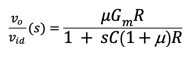
One can then draw a comparison between this equation and the one-pole model of the frequency response for the op amp given in Eq. 2.1 and deduce the following: A0 = u Gm R and wb = 1 / C ( 1 + u) R. Multiplying these together results in the gain-bandwidth product wt given by
(2.4)
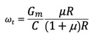
Since usually u >> 1,
(2.5)
![]()
A PSpice Large-Signal Op Amp Subcircuit
Combining the nonlinear effects described above, together with the op amp limited frequency response behavior, we can create a subcircuit description for the op amp that is valid under both large and small signal conditions. Of course, we shall make use of the op amp equivalent circuit shown in Fig. 2.25.
Consider an op amp characterized by a DC gain of 2.52 x 10⁵ V/V, a unity-gain frequency of 1 MHz, and a slew-rate of 0.633 V/ms. Furthermore, we shall assume that the internal compensation capacitor C is 30 pF and that the op amp output stage saturates at ±10 V. Now, it has been shown by Sedra and Smith 3rd Edition that the slew-rate of an op amp is related to the transconductance stage current limit Imax and the capacitor C according to
(2.6)
![]()
Thus, for this particular op amp example, Imax is limited to 19 mA. Likewise, the transconductance of the first stage is simply deduced from Eqn. (2.5) above to be 0.19 mA/V. The remaining two parameters m and R are now left to be determined. Unfortunately, they cannot be uniquely determined from the information provided. We shall assume R=2.5 x 10⁶ W and derive m from A0=m Gm R to get m= 529 V/V.
A subcircuit capable of capturing both the small- and large-signal behavior of the op amp described above is listed below (Refer to Fig. 2.25):
.subckt large_signal_opamp 1 2 3* connections: | | |* output | |* +ve input |* -ve inputR 4 0 2.5MegC 4 5 30pGinput 4 0 Table {V(2)-V(3)} = (-0.1V,-19uA) (+0.1V,19uA)Emiddle 5 0 4 0 -529Eoutput 1 0 Table {V(5)} = (-10V,-10V) (10V,10V).ends large_signal_opamp |
2.4 The Effects of Op Amp Large-Signal Nonidealities On Closed-Loop Behavior
Now that we have created a subcircuit for the op amp that accounts for several of its nonidealities, let us explore some of the idiosyncrasies of the op amp in various closed-loop configurations.
2.4.1 DC Transfer Characteristic of An Inverting Amplifier
Consider the inverting amplifier circuit first shown in Fig. 2.2 with resistors R1=1 k-ohm and R2=10 k-ohm. Let us calculate the DC transfer characteristic of this circuit using PSpice assuming that the op amp is nonideal and modeled as described above in the last section for large signal operation. The PSpice input file is given in Fig. 2.27.
|
Fig. 2.2 The inverting amplifier circuit. (duplicate)
|
DC Transfer Characteristics Of An Inverting Amplifier With Gain -10
* op-amp subcircuit .subckt large_signal_opamp 1 2 3 * connections: | | | * output | | * +ve input | * -ve input R 4 0 2.5Meg C 4 5 30p Ginput 4 0 Table {V(2)-V(3)} = (-0.1V,-19uA) (0.1V,19uA) Emiddle 5 0 4 0 -529 Eoutput 1 0 Table {V(5)} = (-10V,-10V) (10V,10V) .ends large_signal_opamp
** Main Circuit ** * signal source Vi 3 0 DC 1V Xopamp 1 0 2 large_signal_opamp R1 3 2 1k R2 2 1 10k ** Analysis Requests ** .DC Vi -15V +15V 100mV ** Output Requests ** .PLOT DC V(1) .probe .end
Fig. 2.27: Spice input deck for calculating the DC transfer characteristic of an inverting amplifier containing a nonideal op amp.
|
The results of the DC sweep calculations are displayed in Fig. 2.28. As can be seen from this graph, input signals of magnitude less than 1 V will experience a signal gain of -10 without distortion as inferred from the slope of the line in this region. Whereas, signal amplitudes exceeding this limit will not be amplified, but instead the output will be held at a constant voltage of ±10 V depending on the sign of the input signal. Thus, linear circuit operation is limited to input signals less than a volt in magnitude.
To see how these transfer characteristics manifest themselves in the time-domain consider applying a sinewave of 400 mV peak amplitude at a 1 kHz frequency to the input of the amplifier and then repeat the same analysis using an input signal that has a signal amplitude larger than the 1-volt limit. In this particular case, we shall use a signal level of 1.1 V peak. We can use the same PSpice input deck as was just used above for calculating the amplifier DC transfer characteristic by replacing the DC source statement for the first case by the following
Vi 3 0 SIN (0 400mV 1kHz),
and by changing the 400-mV parameter to 1.1 V for this new case. Also necessary is that a transient analysis command replace the DC sweep command statement such as the following
.TRAN 10u 5ms 0s 10u.
The results of these two transient analyses are shown in Fig. 2.29. Clearly, when the input level exceeds the 1 V limit, the output signal becomes clipped. Whereas, the other signal is amplified without any distortion.
|
Fig. 2.28: DC transfer characteristic of the inverting amplifier as calculated by Spice.
|
Fig. 2.29: Evidence of output voltage clipping when the input signal level is too high. |


2.4.2 Slew-Rate Limiting
Another important phenomenon caused by internal amplifier saturation effects is that of slew-rate limiting. This effect plays an important role in determining the high-frequency operation of op amp circuits. To obtain a better understanding of this effect, let us simulate a commonly used experimental set-up for characterizing op amp slewing. This set-up consists of an op amp in a unity-gain configuration and a generator supplying a voltage step as an input signal. The reader first encountered this configuration in Fig. 2.12 of Section 2.2.3, albeit the signal source was a sinewave generator instead of a of PWL generator. We shall use exactly the same large-signal op amp subcircuit developed in the last section; however, we shall add additional terminals to the op amp subcircuit so that we may monitor the output current of the first stage. As we shall see, op amp slew-rate behavior is fully explained by the behavior of this current.
For the first part of our simulation, consider applying a very small step input of 1 mV and observe the transient response at the output of the amplifier and the current that flows between the first and second stages. The PSpice input file is listed below in Fig. 2.30 and the results are displayed in Fig. 2.31(a). The top curve of Fig. 2.31(a) displays both the step input voltage signal and the corresponding output response, the curve below it represents the voltage appearing between the input terminals of the amplifier, and the bottom curve represents the output current of the first stage. As is evident, the output voltage signal increases towards its final state in an exponential manner. Similarly, the voltage appearing between the input terminals of amplifier and the output current of the first stage follows a similar exponential pattern. Moreover, we see that these two signals are proportional to one another; albeit with a negative sign. These results are expected of an op amp whose dynamic behavior is modeled as a single-time-constant network.
|
Circuit setup for Slew-Rate Limiting Investigation.
|
Investigating Op-Amp Slew-Rate Limiting
* op-amp subcircuit .subckt large_signal_opamp 1 2 3 6 4 * connections: | | | | | * output | | \ / * +ve input | | * -ve input | * current monitor of 1st stage Iopen1 2 0 0A ; redundant connection made at +ve input terminal Iopen2 3 0 0A ; redundant connection made at -ve input terminal R 4 0 2.5Meg C 4 5 30p Ginput 6 0 Table {V(2)-V(3)} = (-0.1V,-19uA) (0.1V,19uA) Emiddle 5 0 4 0 -529 Eoutput 1 0 Table {V(5)} = (-10V,-10V) (10V,10V) .ends large_signal_opamp
** Main Circuit ** * signal source Vi 2 0 PWL (0,0V 1us,0V 1.01us,1mV 1s,1mV ) Xopamp 1 2 1 4 5 large_signal_opamp Vmonitor 4 5 0
** Analysis Requests ** .TRAN 10ns 5us 0s 10ns ** Output Requests ** .PLOT TRAN V(2) V(1) I(Vmonitor) .probe .end
Fig. 2.30: Spice input deck for investigating op amp slew-rate limiting.
|

|
(a) a small input voltage step of 1 mV. |
(b) a large input voltage step of 1 V.
|


Fig. 2.31: Input and output waveforms of the unity-gain amplifier when both a small and large voltage step input is applied. The middle curve of each graph is the voltage between the two input terminals of the op amp. Also shown in the lower curve of each graph is the current supplied by the front-end transconductance stage.
Conversely, if a 1 V step input is applied to the input terminal, then instead of an exponential increase in the output voltage, the output voltage ramps up at a constant rate as shown in the top graph of Fig. 2.31(b). This rate, of course, is the slew-rate of the op amp at 0.633 V/ms. To help understand this effect, refer to the voltage and current waveforms shown in the two graphs below the top one. We see from the graph of the current waveform (bottom-most graph) that, for the most part, it is saturated at a constant level of -19 mA, which, of course, is the maximum current deliverable by the first stage i.e. Imax. It is not before the voltage between the input terminals of the op amp (middle graph) goes between ±Imax/Gm or ±100 mV does the transconductance stage enter its linear region and that the current generated by this stage begins to decrease at an exponential rate.
In terms of sinusoidal inputs, slew-rate limiting manifests itself in the output as a distorted sinewave. Consider applying a 100 kHz sinewave of 1.5 V amplitude to the input of the unity-gain buffer described above in the PSpice input file listed in Fig. 2.30. This requires that one change the step input statement to a sinewave input using the following source statement:
Vi 2 0 SIN (0 1.5V 100kHz).
The results of the PSpice simulation are illustrated in Fig. 2.32. In addition to the input and output voltage waveforms, and the evidence of distortion in the output signal, the cause of this distortion should be clear from the waveform of the current signal delivered by the front-end transconductance stage. Under small-signal conditions, this current waveform should be sinusoidal like the input, but, obviously, the front-end stage is being push beyond its linear capability.
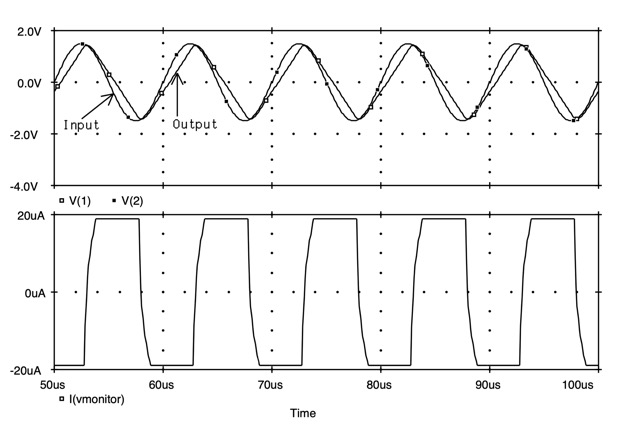
Fig. 2.32: The upper two curves are the input and output waveforms of the unity-gain amplifier subjected to a 100 kHz sinusoidal input signal of 1.5 V amplitude. The lower waveform is of the current being supplied by the front-end transconductance stage.
2.4.3 Other Op Amp Nonidealities
A practical op amp deviates from its ideal behavior in many other ways than those just discussed. Some of these additional nonidealities would include common-mode signal gain, finite input impedances, nonzero output impedance and, DC bias and offset signals. Problems at the end of the chapter illustrates some of these effects. We encourage our readers to attempt some of these.
2.5 Other Op Amp Nonidealities
A practical op amp deviates from its ideal behavior in many other ways than those discussed previously. Some of these additional nonidealities would include common-mode signal gain, finite input impedances, nonzero output impedance and, DC bias and offset signals. In this section we shall demonstrate how to incorporate these nonidealities into circuit simulation using Spice.
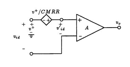
Fig. 3.33: Accounting for the common-mode signal gain of an op amp circuit by attaching a dependent voltage source in series with the positive terminal of the op amp.
2.5.1 Common-Mode Gain
Accounting for op amp common-mode gain is accomplished by simply adding a dependent voltage source in series with the positive input terminal of the op amp, as shown in Fig. 2.33. The op amp shown in Fig. 2.33 can be represented either by an ideal op amp model or one that captures more of its true-life small- and large-signal behavior.
As an example of common-mode signal error, we shall return to the instrumentation amplifier example discussed in section 2.2.4 and assume that the op amps have a finite common-mode rejection ratio (CMRR). Recall that CMRR is defined as the ratio of the op amp differential gain to the corresponding common-mode gain. The rest of the circuit will be assumed ideal and perfectly matched. Thus, under ideal op amp conditions, common-mode signals appearing at the input of the instrumentation amplifiers should not appear at its output. However, some common-mode signal will appear at the output and we wish to determine the magnitude of this signal when the op amps have an assumed CMRR of 80 dB and a finite DC gain of 120 dB. The Spice input deck for this particular example is identical to the one used in section 2.2.4, and listed in Fig. 2.18, except that the op amp subcircuit ideal_opamp is replaced with the following one:
|
.subckt common_mode_opamp 1 2 3 * connections: | | | * output | | * +ve input | * -ve input Iopen1 2 0 0A Iopen2 3 0 0A Iopen3 4 0 0A Eerror 2 4 4 0 100u ; Gain = 1/CMRR Eamp 1 0 4 3 1e6 .ends common_mode_opamp
|
The Spice results are shown in Fig. 2.34 and show that a 2.5 mV 60 Hz signal component appears at the output. Thus, this instrumentation amplifier has a common-mode voltage gain (ACM) of 2.5 mV / 25 V, or 10-4 V/V. Combining this with the result found previously for the differential gain (Ad) of 420 mV / 20 mV, or 21 V/V, we can compute the overall CMRR for this instrumentation amplifier to be 21 V/V / 10-4 V/V or 106 dB.
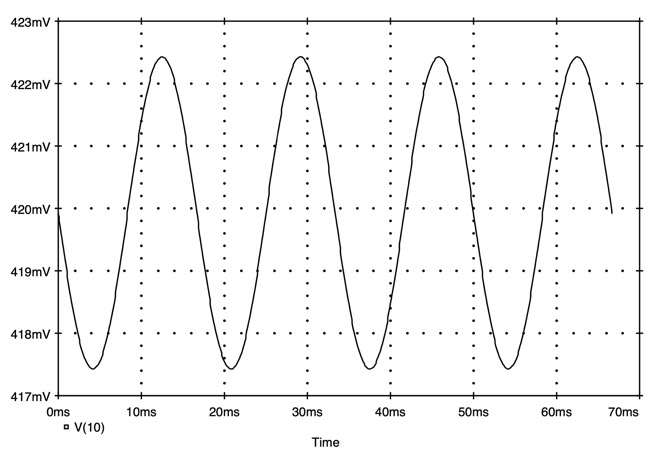
Fig. 2.34: Common-mode signal feeding through from the input of the instrumentation amplifier to its output because of the finite CMRR of the op amp.
2.5.2 Input and Output Resistances
Input and output impedances can be added to the op amp subcircuit in a straightforward way. We encourage the reader to try and incorporate input and output resistors for the various op amp models presented above. On completion, calculate the input and output impedance of some closed-loop op amp circuit as a function of frequency. The results should prove interesting.
Also note that many of the redundant connections made by the zero-valued current sources in these subcircuits will no longer be needed once the input and output resistances are added. They can therefore be removed to simplify the subcircuit.
2.5.3 DC Problems
Consider the equivalent circuit for the op amp shown in Fig. 2.35 which is separated into two parts: the first part consists of a set of input-referred DC signal sources representing the offsets and bias currents of the op amp, and the second part consists of an op amp circuit free of any DC offsets or bias currents. The two current sources labeled IB represent the average value of the DC current flowing into the op amp input terminals. The polarity of these sources will depend on the front-end nature of the amplifier, i.e., positive for front-end npn transistors and negative for a pnp transistorized front-end. The current source IOS represents the difference between the actual currents that flow into the op amp input terminals. The voltage source VOS represents the input-referred offset voltage. A subcircuit taking into account these bias and offset signals is listed below:
|
.subckt dc_opamp 1 2 3 * connections: | | | * output | | * +ve input | * -ve input IB1 4 0 DC 200nA IB2 3 0 DC 200nA IOS/2 3 4 DC 5nA VOS 4 2 DC 5mV Xdc_free_opamp 1 4 3 ideal_opamp .ends dc_opamp
|
Here we have specified that the op amp will have an input-referred offset voltage of +5 mV, an input bias current of 200 nA and an offset current of 5 nA. Notice that we are calling the previously defined op amp subcircuit named ideal_opamp inside this new subcircuit. This form of nesting subcircuit calls is valid provided each subcircuit is found within the Spice input file. But note that a subcircuit cannot be made to call itself.
|
Fig. 2.35: Modeling the effect of op amp DC offsets. Here we have included a DC voltage source in series with the positive input terminal of the op amp to account for its voltage offset, two equal current sources connected to the input terminals of the ideal op amp to account for its input bias currents, and a third current source to account for the input offset current.
Fig. 2.2 The inverting amplifier circuit. (duplicate)
|
The Effect Of DC Offsets On A Miller Integrator
* op-amp subcircuits
.subckt ideal_opamp 1 2 3 * connections: | | | * output | | * +ve input | * -ve input Iopen1 2 0 0A Iopen2 3 0 0A Eoutput 1 0 2 3 1e6 .ends ideal_opamp
.subckt dc_opamp 1 2 3 * connections: | | | * output | | * +ve input | * -ve input IB1 4 0 DC 200nA IB2 3 0 DC 200nA IOS/2 3 4 DC 5nA VOS 4 2 DC 5mV Xdc_free_opamp 1 4 3 ideal_opamp .ends dc_opamp
** Main Circuit **
* inverting amplifier Vi 3 0 DC 0 Xopamp 1 0 2 dc_opamp R1 3 2 1k C2 2 1 10uF ** Analysis Requests ** .TRAN 500ms 10s 0s 500ms UIC ** Output Requests .PLOT TRAN V(1) .probe .end
Fig. 2.36: A Spice input file for calculating the effect of op amp DC offsets on integrator output when the input is set to zero. Since no initial conditions are explicitly indicated, Spice assumes that all nodes are initially at 0 V.
|

Given the above model accounting for DC offset effects, let us consider the effect that these offsets have on integrator behavior. Returning to the Spice input file for the Miller integrator shown in Fig. 2.5, we have modified it to include the above described op amp model, as shown in Fig. 2.36. A transient analysis request is included in this file. An additional UIC (use initial conditions) flag is included on this analysis request in order to ensure that the transient analysis begins with all nodes in the integrator circuit at 0 V. Without UIC, the transient analysis would begin with the nodes set at their DC operating point which turns out to be the final conditions of the transient analysis[3].
The results of the transient analysis are shown in Fig. 2.37. We see here that even though the input to the integrator is zero, its output ramps upwards towards the positive power supply; clearly, an undesirable situation. In practise, one usually finds that eventually the op amp output voltage reaches the positive saturation level of the op amp. We would not see this here since our op amp does not model output voltage saturation effects. But, of course, this could easily be included by replacing the ideal op amp model with one that accounts for op amp large-signal behavior, such as the one described in Section 2.3.2.
A practical method commonly used to eliminate this run-away effect is to connect a resistor across the integrator capacitor. Consider adding a 100 kW resistor across C2. This requires that we add the following Spice statement to the Spice deck listed in Fig. 2.36:
R2 1 2 100k.
If we run the revised Spice file and observe the voltage that appears at the integrator output, one would find the voltage signal shown in Fig. 2.38. Here we do not see the output voltage increase without bound, but rather, exponentially settle to a constant output signal of about 526 mV. This is the net output offset voltage of the integrator. This value can easily be calculated by hand analysis.
|
Fig. 2.37: The effect of op amp DC offsets on the Miller integrator output when the input is grounded.
|
Fig. 2.38: The effect of op amp DC offsets on the Miller integrator output when the input is grounded but the feedback capacitor is shunted with a 100 k-ohm damping resistor.
|


2.6 Spice Tips
· An ideal op amp can be modeled as a voltage-controlled voltage source with a large DC gain of at least 106 V/V.
· Nodes that do not have a DC path to ground are considered as floating nodes. Spice will not run with floating nodes. To circumvent this problem, connect large resistors between each floating node and ground.
· At least 2 or more connections must be made at each node in a circuit in order for Spice to run. Situations often arise when using controlled sources that this condition is violated. One can get around this problem by either connecting a large resistor between the node in question and ground, or by connecting a zero-valued current source between the node in question and ground. The latter method has the advantage that it does not disturb the operation of the network in any way.
· To simplify the writing of Spice input files, subcircuits of basic building blocks of the main circuit can be used to separate different portions of the circuit into smaller, more manageable, circuit blocks.
· When concatenating several Spice decks together into one file there cannot be any blank lines that separate the end of one Spice deck (denoted by an .end statement) from the start of another Spice deck.
· Newer versions of Spice have the capability of describing the terminal behavior of a dependent source in either functional or piecewise-linear form. This is known as analog behavior modeling and provides a very elegant means of describing circuit behavior to Spice.
· The initial conditions of a transient analysis can come from three sources: (1) DC operating point, (2) all node voltages and branch currents assumed 0, or (3) predefined initial conditions. One should be aware of the initial conditions used by Spice during a transient analysis so that the results are meaningful.
· As a general rule, when performing a transient analysis of a circuit that does not contain any time-varying sources, a UIC (use initial conditions) command should be included on a .TRAN statement.
2.7 Bibliography
1. Staff, PSpice Users' Manual, MicroSim Corporation, Irvine, California, Jan. 1991.
2.8 Problems
2.1. Assuming a pseudo-ideal op amp model for each op amp (i.e., DC gain of 106), determine, with the aid of Spice, the voltage gain vo/vi and input and output resistance of each of the circuits in Fig. P2.1.
2.2. Design an inverting op amp circuit for which the gain is -4 V/V and the total resistance used is 100 k-ohm. Verify your design using Spice.
2.3. Repeat Problem 2.1 for the case the op amps have a finite gain A=1000.
2.4. A Miller integrator incorporates an ideal op amp, a resistor R of 100 k-ohm and a capacitor C of 0.1 uF. Using the AC analysis capability of Spice, together with the ideal op amp represented by a high-gain VCVS, determine the following:
(a) At what frequency are the input and output signals equal in amplitude?
(b) At this frequency how does the phase of the output sinewave relate to that of the input?
(c) If the frequency is lowered by a factor of 10 from that found in (a), by what factor does the output voltage change, and in what direction (smaller or larger)?
(d) What is the phase relation between the input and output in situation (c)?
Confirm each of these situations by applying a 1-V peak sinewave at the appropriate frequency and compare the voltage waveform appearing at the output using the transient analysis of Spice.
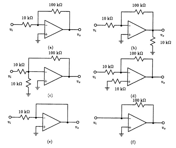
Fig. P2.1
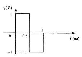
Fig. P2.5
2.5. A Miller integrator whose input and output voltages are initially zero and whose time constant is 1 ms is driven by the signal shown in Fig. P2.5. Using Spice compute the output transient waveform that results. Repeat the above simulation with the input levels increased to ±2 V and the time constant raised to 2 ms. How does this output compare to that when the time constant is 1 ms?
2.6. Consider a Miller integrator having a time constant of 1 ms, and whose output is initially zero, when fed with a string of pulses of 10-ms duration and a 1 V amplitude rising from 0 V (see Fig. P2.6). Use Spice to obtain a plot of the output voltage waveform. How many pulses are required for an output voltage change of 1 V?
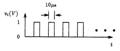
Fig. P2.6
2.7. In order to limit the low-frequency gain of a Miller integrator, a resistor is often shunted across the integrating capacitor. Consider the case when the input resistor is 100 k-ohm, the capacitor is 0.1 uF, and the shunt resistor is 10 M-ohm.
(a) Use the AC analysis capability of Spice to compute the Bode plot of the magnitude response of the resulting circuit and contrast it with that of an ideal integrator (that is, without the shunt resistor). At what frequency does the circuit begin to behave less as an integrator and more as an amplifier?
(b) Use the transient analysis capability of Spice to obtain a plot of the output voltage waveform resulting when an input pulse of 0.1 V height and 1 ms duration is applied. Consider the cases without and with the shunt resistor.
2.8. A differentiator utilizes a pseudo-ideal op amp, a 10 k-ohm resistor, and a 0.01 uF capacitor. Using the AC analysis command of Spice, determine the frequency fo at which its input and output sinewave signals have equal magnitude. What is the output signal for a 1 V peak-to-peak sinewave input with frequency equal to 10fo?
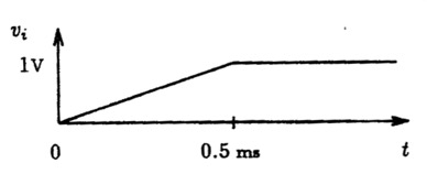
Fig. P2.9
2.9. An op amp differentiator with a 1 ms time constant is driven by the rate-controlled step shown in Fig. P2.9. Initializing the output voltage at 0 V, compute the voltage time waveform that appears at the output using Spice over a time interval of at least 5 ms.
2.10. A weighted summer circuit using a pseudo-ideal op amp has three inputs using 100 kW resistors and a feedback resistor of 50 k-ohm. A signal v1 is connected to two of the inputs, while a signal v2 is connected to the third. With the aid of Spice, determine the output voltage vo if v1=3 V and v2=-3 V.
2.11. Design an op amp circuit to provide an output vo=-( 3 v1 + v2/2 ). Choose relatively low values of resistors but ones for which the input current (from each input signal source) does not exceed 0.1 mA for 2 V input signals. Verify all attributes of your design using Spice.
2.12. In an instrumentation system, there is a need to take the difference between two signals, one being, v1= 3 sin( 2p x 60 t) + 0.01 sin( 2p x 1000 t) volts, and another, v2 = 3 sin( 2p x 60 t) - 0.01 sin( 2p x 1000 t) volts. Design a difference amplifier that meets the above requirements using two op amps. In addition, amplify the resulting difference by a factor of 10. Verify your design using Spice by simulating the transient behavior of your circuit. Plot both the input and output signals. Model each op amp with a high-gain VCVS.
2.13. It is required to connect a 10 V source with a source resistance of 100 k-ohm to a 1 k-ohm load. Find the voltage that will appear across the load if:
(a) the source is connected directly across the load.
(b) an op amp unity-gain buffer is inserted between the source and load.
In each case, find the load current and the current supplied by the source. Also, monitor the current supplied by the op amp. Assume that the op amp is pseudo-ideal with a DC gain of 106.
2.14. Consider the instrumentation amplifier of Fig. 2.15 with a common-mode input voltage of +5 V (dc) and a differential input signal of 10 mV peak, 1 kHz sinewave. Let R1=1 k-ohm, R2=0.5 M-ohm, and R3=R4=10 k-ohm. With the aid of Spice, plot the voltage waveform at each node in the circuit for at least 2 periods of the input signal.
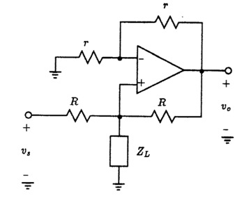
Fig. P2.15
2.15. For the negative impedance converter circuit of Fig. P2.15 with R=1 k-ohm and vs =1 V, use Spice to determine the voltages across the load and at the output of the op amp, for load resistances of 0 ohm, 100 ohm, 1 k-ohm and 2 k-ohm.
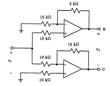
Fig. P2.16
2.16. The circuit shown in Fig. P2.16 is intended to supply current to floating loads while making greatest possible use of the available power supplies. With a 1 V peak-to-peak, 1 Hz sinewave applied to its input, plot the voltage waveform appearing at nodes B and C. Also, plot vo. What is the voltage gain vo / vi?
2.17. Measurements performed on an internally compensated op amp shows that at low frequencies its gain is 4.2 x 10⁴ V/V and has a 3-dB frequency located at 100 Hz. Create a small-signal equivalent circuit model of this op amp and verify using the AC frequency analysis of Spice that it satisfies the above measurements.
2.18. A noninverting amplifier with a nominal gain of +20 V/V employs an op amp having a DC gain of 104 and a unity-gain frequency of 106 Hz. Model this behavior using an equivalent circuit, and with the aid of Spice, plot the magnitude response of the closed-loop amplifier and determine its 3-dB frequency f3dB. What is the gain at 0.1 f3dB and at 10 f3dB?
2.19. Consider a unity-gain follower utilizing an internally compensated op amp with ft=1 MHz. Assume that the low frequency gain is 106 V/V. Using Spice, determine the 3-dB frequency of the follower by plotting the magnitude response of the follower using the AC analysis command. At approximately what frequency is the gain of the follower 1% below its low frequency magnitude. What is the corresponding phase shift at this frequency? If the input to the follower is a 1 V step, determine the 10% to 90% rise time of the output voltage using the transient analysis command of Spice.
2.20. Consider an inverting summer with two inputs V1 and V2 and with Vo = -(V1 + V2). With the aid of Spice, determine the 3-dB frequency of each of the gain functions Vo/V1 and Vo/V2 assuming that the small-signal behavior of the op amp is modeled after the 741 op amp. How do they compare with that predicted by theory? (Hint: In each case, the other input to the summer can be set to zero.)
2.21. A Miller integrator uses a 100 kW input resistor and a feedback capacitor of 0.1 uF. Using Spice, compare the magnitude and phase response of this Miller integrator assuming that the op amp is: a) pseudo-ideal, and b) internally compensated with a dc gain of 105 V/V and a 3 dB frequency of 10 Hz. For comparison purposes, its easiest to concatenate the two Spice files together and submit them together as one file to Spice. In this way, the results of the two situations can be directly compared. What is the ``excess phase’’ that the nonideal integrator has at the unity-gain frequency of the (pseudo-)ideal integrator? Is the excess phase of the lag or lead type?
2.22. A particular family of op amps has an internal structure that can be modeled as that in Fig. 2.25. Four separate designs are being considered that have the following small-signal parameters:
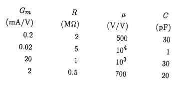
Create a Spice subcircuit that captures the above four circuit descriptions and then use it to plot the input-output voltage gain as a function of frequency. What is the DC gain, 3 dB and unity-gain frequencies for each op amp?
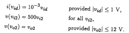
2.23. Consider that the large-signal behavior of an internally compensated op amp can be modeled as that shown in Fig. 2.25. Assume that the resistor R has a 1 M-ohm value, capacitor C is 30 pF and the three control sources are described by the following mathematical expressions:
Create a Spice (PSpice) subcircuit that captures the above behavior and verify that it indeed satisfies the given descriptions. Next, connect the op amp in a unity-gain configuration and apply a 5 V step input. Compute the expected output transient response and determine the positive-going slew-rate for this amplifier. How does this value compare with that predicted by theory?
2.24. For the large-signal op amp described above in Problem 2.23, use Spice to compute the magnitude response for this amplifier as a function of frequency between 0.1 Hz and 100 MHz. What is the corresponding DC gain, 3 dB and unity-gain frequencies?
2.25. Consider an inverting amplifier configuration having a gain of -10. Using the large-signal op amp model described in Section 2.3, confirm that the highest frequency of a 15 V peak-to-peak sinewave that passes undistorted through the amplifier is 13.5 kHz. Do this by having Spice (PSpice) compute the transient behavior of the amplifier subject to the 1.5 V peak-to-peak input sinewave of 13.4 kHz and compare this result to that when the frequency of the input signal is increased to 13.6 kHz.
2.26. To demonstrate the many trade-offs that a designer faces when designing with op amps, consider investigating the limitations imposed on a noninverting amplifier having a nominal gain of 10 with an op amp that has a unity-gain bandwidth (ft) of 2 MHz, a slew rate (SR) of 1 V/ms and an output saturation voltage (Vomax) of 10 V. Model the op amp using the large-signal macromodel described in Section 2.3. Assume a sinewave input with peak amplitude Vi.
(a) If Vi =0.5 V, what is the maximum frequency of the input signal that can be applied to this amplifier before the output signal shows visible distortions?
(b) If the frequency of the input signal is 20 kHz, what is the maximum value of Vi before the output distorts?
(c) If Vi =50 mV, what is the useful frequency range of operation?
(d) If f=5 kHz, what is the useful input voltage range?
2.27. An op amp with a DC gain of 106 V/V and a CMRR of only 40 dB is used in a noninverting configuration with a closed-loop gain of 2. Model the behavior of this op amp using a Spice subcircuit consisting of several VCVSs. Plot the voltage waveform that appears at the output of the amplifier when an input signal wave of 1 kHz and 10 V peak-to-peak is applied to this amplifier configuration.
2.28. A particular op amp, for which A0=104, RiCM=10 M-ohm, and Rid = 10 k-ohm, is connected in the noninverting configuration with a closed-loop gain of 10 (ideally). Model the op amp with a VCVS, then, with the aid of Spice, determine the input resistance seen by the source for low frequencies?
2.29. An op amp for which RiCM = 50 M-ohm, Rid=10 k-ohm, A0=104, and ft=106 Hz is used to design a noninverting amplifier with a nominal closed-loop gain of 10. Model the op amp with a single pole small-signal equivalent circuit model and create a Spice subcircuit for it before arranging the resistor feedback around it. With the aid of the AC analysis capability in Spice, apply a 1 V AC voltage signal to the amplifier input and plot the magnitude of the admittance seen by this source over a frequency interval of 0.1 Hz to 107 Hz.
2.30. An inverting amplifier for which R1=10 k-ohm and R2=100 k-ohm is constructed with an op amp whose open-loop output resistance is 1 k-ohm, whose dc gain is 104, and whose 3-dB frequency is 100 Hz. Evaluate the magnitude of the output impedance of the closed loop amplifier over a frequency interval of 0.01 Hz to 107 Hz. Select a logarithmic sweep of the input signal frequency.
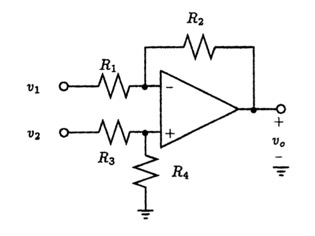
Fig. P2.32
Fig. P2.33
2.31. A noninverting amplifier with a gain of 100 uses an op amp having an input offset voltage of ±2 mV. Assume that the rest of the op amp can be modeled as a high-gain VCVS. If a 10-mV peak sinewave of 1 Hz frequency is applied to the input of the amplifier, observe the voltage waveform that appears at the amplifier output using Spice.
2.32. Consider the differential amplifier circuit in Fig. P2.32. Let R1=R3=10 k-ohm and R2=R4=1 M-ohm. If the op amp has VOS = 3 mV, IB=0.2 uA, and IOS=50 nA, determine, with the help of Spice, the dc offset voltage that appears at the amplifiers output. Assume that the rest of the op amp is pseudo-ideal (i.e., modeled as a high-gain VCVS).
2.33. The circuit shown in Fig. P2.33 uses an op amp that has a ±5 V offset. Assume that the op amp is pseudo-ideal except for the dc offset. Determine the output offset voltage using Spice. What does the output offset become with the input ac coupled through a 1 uF capacitor? If, instead, the 1 k-ohm resistor is capacitively coupled to ground, what does the output offset become?
2.34. An op amp is connected in a closed loop with gain of +100 utilizing a feedback resistor of 1 M-ohm. With the aid of Spice, answer the following:
(a) If the input bias current is 100 nA and everything else about the op amp is assumed ideal, what output voltage results with the input grounded?
(b) If the input offset voltage is ±1 mV, and the input bias current as in (a), what is the largest possible output that can be observed with the input grounded?
(c) If bias current compensation is used, what is the value of the required resistor? Verify that this indeed reduces the output offset voltage.
[1] Spice version 2G6 and later have a built-in command called .ALTER that allows the user to specify changes to the circuit without having to re-type the entire file as we do here. Unfortunately, the student version of PSpice does not have this command or one that accomplishes the same thing, so we have opted to re-create a new Spice deck for each circuit change and concatenate them together into one file for processing. In this way, we can view the results together using Probe.
[2] Study of this section relies heavily on the analog behavior modeling feature of PSpice. Those readers who do not have access to a version of Spice equipped with this feature can still perform the op amp simulations presented here provided the op amp macromodel present in Section 12.1 is substituted for the op amp subcircuit developed in this section; albeit with the appropriate modifications to the subcircuit call.
[3] When calculating the transient behavior of a circuit that contains no time-varying voltage or current sources, a UIC command should always be included on the .TRAN statement. In this way, the DC operating point of the circuit will not be used as the initial condition for the circuit.} The input to the integrator is set to zero in order for us to observe separately the effect of op amp offsets.